
SiC-Coated Graphite Susceptors for GaN MOCVD: Engineering & Procurement Guide
Master the procurement and design of SiC-coated graphite susceptors for GaN MOCVD. Learn how CTE matching, pocket design, and coating purity impact wafer yield.
As Gallium Nitride (GaN) power electronics and RF devices rapidly scale from niche applications to high-volume automotive and 5G infrastructure markets, the demands on epitaxial growth processes have never been higher. Metal-Organic Chemical Vapor Deposition (MOCVD) remains the dominant method for growing high-quality GaN layers on Si, SiC, or Sapphire substrates. At the very heart of this process lies the SiC-coated graphite susceptor—the critical thermal and mechanical interface between the chamber heaters and the semiconductor wafer.
For procurement teams and process engineers, specifying and sourcing these susceptors is a high-stakes decision. A poorly designed pocket, a mismatched Coefficient of Thermal Expansion (CTE), or a micro-crack in the SiC coating can lead to catastrophic yield loss, wafer bowing, and premature chamber downtime.
This guide provides a comprehensive engineering and procurement framework for SiC-coated graphite susceptors in GaN MOCVD applications. It covers environmental challenges, structural design, quality control, and total cost of ownership (TCO) optimization.
Executive Summary
- The Core Function: SiC-coated graphite susceptors provide uniform heating while protecting the porous graphite core from the highly corrosive ammonia (NH₃) and metal-organic precursors used in GaN epitaxy.
- Critical Failure Modes: The most common reasons for susceptor replacement are SiC coating delamination (due to CTE mismatch), pinhole propagation, and dimensional drift in the wafer pocket.
- Yield Impact: Pocket geometry directly controls the thermal gradient across the wafer, dictating the GaN layer thickness uniformity and minimizing thermally induced slip lines.
- Update Status: Last verified on July 27, 2026, for global GaN MOCVD procurement and process-engineering review.
Scope, Date, and Decision Boundary
This guide was last checked on July 27, 2026 for global procurement managers, epitaxy process engineers, and equipment OEM teams specifying SiC-coated graphite susceptors for GaN MOCVD programs. It is most relevant to GaN-on-Si, GaN-on-SiC, and sapphire LED or HEMT production where wafer temperature uniformity, coating integrity, and contamination control drive yield.
The guidance applies to CVD SiC-coated isostatic graphite wafer carriers and susceptors. It does not cover solid SiC carriers, TaC-coated PVT hot-zone hardware, quartzware, or generic vacuum-furnace graphite trays. Treat the specification ranges below as RFQ screening bands, not final release criteria. Before production use, align drawings, coated-part CMM reports, coating inspection evidence, and dummy-wafer qualification data with your chamber owner. For broader material fit, compare the chamber environment with the semiconductor thermal-field solution guide and material compatibility matrix.
1. The Harsh Reality of GaN MOCVD Environments
Growing GaN requires a distinctly hostile environment compared to standard silicon epitaxy. The process involves cracking Trimethylgallium (TMGa) and Ammonia (NH₃) at extreme temperatures to form the GaN crystal structure.
High-Temperature Extremes
GaN MOCVD typically operates at temperatures between 1,000°C and 1,150°C for the active growth phases, and can exceed 1,200°C during chamber baking/cleaning cycles. At these temperatures, conventional metals soften or melt, and many ceramics suffer from thermal shock. Graphite is one of the few materials that actually increases in strength at these temperatures while providing excellent thermal conductivity.
The Corrosive Attack of Ammonia
Ammonia is highly reactive at 1,000°C. If bare graphite is exposed to hot NH₃ and hydrogen carrier gases, it undergoes severe methanation and localized etching. This reaction rapidly degrades the graphite, generating hydrocarbon contaminants and carbon particulate dust ("dusting") that will immediately ruin the GaN epitaxial layer.
The Chemical Vapor Deposition (CVD) Silicon Carbide coating acts as an ultra-hard protective barrier. When the coating remains dense and intact, it seals the graphite core, provides high resistance against NH₃, TMGa, and typical cleaning gases like HCl or Cl₂, and sharply reduces outgassing and particulate shedding risk. For standard coated carrier families, review the CVD SiC-coated susceptor product path before issuing a custom RFQ.
2. Anatomy of a High-Yield SiC-Coated Susceptor
A premium SiC-coated graphite susceptor is not a simple commodity; it is a highly engineered composite material consisting of three critical zones:
- The Isostatic Graphite Core: The foundation must be ultra-fine grain, isostatically pressed graphite. It dictates the overall thermal conductivity and mechanical strength. High purity (ash content < 5 ppm) is mandatory to prevent metallic ions (like Iron or Copper) from migrating outward at high temperatures.
- The Interfacial Boundary: This is where the SiC coating bonds to the graphite. If the graphite surface is not properly prepared, or if the CTE between the graphite and the SiC is not perfectly matched across the entire operating temperature range, sheer stress will accumulate here during rapid heating/cooling cycles.
- The CVD SiC Coating: A dense, stoichiometric (1:1 Si:C ratio) crystalline layer, typically 50 µm to 150 µm thick. It must be free of pinholes, micro-cracks, and nodules.
Figure 1: Cross-sectional architecture of a SiC-coated graphite susceptor in an MOCVD chamber, illustrating the protective coating barrier and pocket design.
3. Engineering Deep Dive: Pocket Design and Wafer Bowing
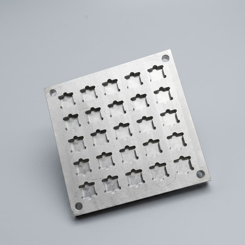
The "pocket" is the recess in the susceptor where the wafer sits. Its geometry is arguably the most critical parameter influencing epitaxial yield. Because GaN has a significant lattice and CTE mismatch with substrates like Silicon, the wafer will naturally bow (warp) during the rapid temperature ramping and growth phases.
If the wafer bows away from the susceptor, the gap between the wafer and the heat source changes, creating severe temperature gradients. A temperature deviation of just 1°C to 2°C across a 200mm wafer can disrupt Indium incorporation in InGaN quantum wells, shifting the emission wavelength of LEDs or degrading the electron mobility in GaN HEMTs.
Pocket Geometry Strategies
- Flat Pockets: Used primarily for smaller, highly rigid substrates (like bulk SiC) where bowing is minimal. They are easier to machine but offer no compensation for severe warpage.
- Spherical / Concave Pockets: Specifically machined with a calculated curvature (often measured in tens of microns of depth). As a GaN-on-Si wafer heats up and becomes convex, it nestles perfectly into the concave pocket, maintaining uniform thermal contact across its entire diameter.
- Stepped / Multi-Zone Pockets: Feature complex edge lips to prevent gas flow underneath the wafer, mitigating edge-cooling effects and preventing premature edge delamination of the GaN film.
Procurement Tip: When auditing suppliers, request their CMM (Coordinate Measuring Machine) data capabilities. A supplier must be able to verify the pocket curvature to within ±5 µm tolerances after the SiC coating has been applied, as the coating process itself can slightly alter the final geometry.
4. CTE Matching: The Silent Killer of Susceptors
The Coefficient of Thermal Expansion (CTE) measures how much a material expands when heated. Silicon Carbide and Graphite inherently expand at different rates. If a susceptor manufacturer simply takes an off-the-shelf block of graphite and coats it with SiC, the resulting component is a ticking time bomb.
During the MOCVD heat-up phase (room temperature to 1100°C in minutes), the graphite core may expand faster than the SiC shell. This places the SiC coating under extreme tensile stress. Because ceramic SiC is brittle, it will develop microscopic spider-web cracks.
Once micro-cracks form:
- Ammonia and Hydrogen penetrate the cracks and attack the graphite.
- The graphite converts to methane gas.
- The gas pressure builds up beneath the coating, blowing a chunk of SiC off the susceptor (delamination).
- The exposed graphite sheds carbon dust, destroying the batch of wafers and requiring a massive chamber wet-clean.
Premium manufacturers solve this by utilizing highly specialized grades of isostatic graphite whose CTE profile is deliberately engineered to identically match the specific CTE of their CVD SiC coating across the 20°C to 1200°C spectrum.
5. Structuring Your RFQ: Key Susceptor Specifications
When procuring SiC-coated graphite susceptors for MOCVD, broad specifications lead to inconsistent batches. Use the following structured table to define exact parameters in your Requests for Quotation (RFQs).
| Specification Parameter | Standard Requirement | Premium / Advanced Node Requirement | Impact on MOCVD Process |
|---|---|---|---|
| Base Graphite Purity | Ash < 20 ppm | Ash < 5 ppm (Halogen Purified) | Prevents metallic ion outgassing at >1000°C; critical for GaN HEMT mobility. |
| Coating Thickness | 50 - 80 µm | 80 - 120 µm (with uniform edges) | Determines lifespan against chemical etching and repeated mechanical handling. |
| Coating Composition | -SiC (Cubic) | Highly oriented -SiC, 99.999% purity | Ensures chemical inertness; resists HCl etching during chamber cleaning cycles. |
| CTE Mismatch Limits | Prevents micro-cracking and catastrophic coating delamination during rapid thermal cycling. | ||
| Pocket Profile Tolerance | Flatness | Controlled curvature (Spherical) | Directly dictates wafer temperature uniformity, eliminating slip lines and wavelength drift. |
| Surface Roughness (Ra) | (Polished options available) | Affects emissivity and how easily wafer handling robots can load/unload without scratching. | |
| Pinholes / Nodules | Zero visual defects | 100% Optical & SEM inspection for zero pinholes | A single pinhole will cause graphite degradation, particle storms, and immediate wafer loss. |
Before releasing a purchase order, map each table row to supplier evidence: material lot traceability, purification certificate, coated-part dimensional report, coating thickness map, and clean packaging record. The acceptance package should follow the same evidence discipline described in our quality and metrology evidence guide.
6. Preventative Maintenance and Total Cost of Ownership
The lowest-cost susceptor is rarely the most economical. In GaN MOCVD, the cost of a ruined epitaxial run (often tens of thousands of dollars in wasted substrates and precursors) dwarfs the price of the susceptor itself.
Service Life Drivers: The lifespan of a susceptor is dictated by how many times it can undergo thermal cycling and chamber cleaning (baking in HCl or Cl₂) before the SiC coating thins out or the pocket dimensions drift out of specification.
TCO Optimization Strategy:
- Track Run-Hours: Implement strict barcode tracking for every susceptor. Correlate epitaxial yield drops (specifically edge uniformity) with the specific susceptor's run-hours.
- Scheduled Replacement: Do not wait for visual delamination. Establish a hard PM replacement limit based on empirical data (e.g., replace after 300 runs). Running a susceptor until it physically fails will cost you far more in chamber recovery time.
- Refurbishment: Ask your supplier about stripping and recoating. If the graphite core remains structurally sound and the pockets haven't drifted, the remaining SiC can sometimes be stripped and a fresh layer applied, recovering 40-60% of the cost of a new susceptor. (See our guide on Susceptor Refurbishment).
7. Engineering & Procurement Checklist
Use this checklist during supplier audits and design reviews to ensure you are sourcing production-ready MOCVD hardware:
- Graphite Sourcing: Can the supplier trace the specific batch/lot of the base isostatic graphite?
- Purification Protocol: Is the graphite halogen-purified after rough machining but before CVD coating to eliminate machining contaminants?
- Coating Uniformity: Does the supplier provide a coating thickness map, especially verifying coverage on sharp edges, lip radii, and gas flow channels?
- Dimensional Verification: Are CMM reports provided for the final, coated part, proving that the pocket curvature meets the required design?
- Defect Inspection: What is the inspection standard for pinholes and nodules? Is UV light or SEM used?
- Packaging: Are the susceptors vacuum-sealed in cleanroom-grade double bags? SiC coatings are hard but brittle; poor shipping practices can induce edge chipping before the part even reaches the fab.
8. Frequently Asked Questions (FAQ)
Q: Why can't we use Solid SiC susceptors instead of coated graphite to avoid delamination entirely? A: While Solid (monolithic) SiC has ultimate purity, it is extremely difficult and expensive to machine. A multi-wafer planetary susceptor has complex pockets, gas grooves, and interlocking features. Machining these into solid SiC is economically unviable. Furthermore, solid SiC has lower thermal conductivity than graphite, which makes achieving the required rapid temperature ramp rates difficult in existing heater setups.
Q: How does the SiC coating thickness affect thermal conductivity? A: SiC has a slightly lower thermal conductivity than the specialized graphite core. If the coating is too thick, it acts as a thermal barrier, slowing down the heat transfer and potentially causing localized hot spots. A thickness of 80–120 µm is the industry sweet spot, balancing robust chemical protection with optimal thermal transparency.
Q: Our wafers are showing slip lines at the edges. Is the susceptor to blame? A: Highly likely. Slip lines are macroscopic crystal defects caused by severe thermal gradients across the wafer. If the wafer pocket is too flat and the wafer bows away at the edges, the edges cool down faster than the center. Redesigning the pocket with a specific concave curvature to match the wafer's high-temperature bow profile is the standard engineering fix.
Q: Can we clean a SiC-coated susceptor with abrasive pads if deposition builds up? A: No. Mechanical abrasion will micro-scratch the SiC coating, creating stress concentration points that lead to cracking during the next thermal cycle. It can also alter the surface emissivity. All cleaning should be done chemically (in-situ gas baking) or through approved wet-clean protocols if removed from the chamber.
9. Conclusion
The transition from R&D GaN growth to high-volume manufacturing requires eradicating every variable that negatively impacts yield. The SiC-coated graphite susceptor is a major variable. By tightly controlling base graphite purity, enforcing strict CTE matching, and engineering precise pocket geometries, fabs can achieve uniform, defect-free GaN epitaxy run after run.
Procurement teams must shift from viewing these susceptors as simple consumables to treating them as highly engineered sub-components that dictate the profitability of the MOCVD tool.
Need Expert Consultation for Your MOCVD Hardware?
Whether you are scaling up GaN-on-Si production for power devices or fine-tuning InGaN LEDs, our engineering team can review drawings, pocket tolerance targets, coating requirements, and clean-pack expectations before quotation. Contact SiC Graphite Technical Sales today to discuss your RFQ requirements.
10. Sources and References
- AIXTRON SE: Product portfolio context for MOCVD platforms used in compound-semiconductor epitaxy. AIXTRON Products
- SGL Carbon: SIGRAFINE® SiC coating specifications, highlighting the protection of isostatic graphite from chemical attack and oxidation in semiconductor processing. SGL Carbon Materials
- Mersen: Advanced materials context for semiconductor manufacturing, high-temperature components, and process-critical material selection. Mersen Semiconductor Solutions
Author

More Posts
Rigid Carbon Felt Insulation for 8-Inch SiC PVT: Rayon vs. Pitch, Outgassing, and Thermal Drift Mitigation
Compare rigid carbon felt insulation for 8-inch SiC PVT: qualify rayon, pitch and PAN grades, outgassing and thermal drift. Build your RFQ evidence checklist.
TaC vs. SiC Coated Graphite for 8-Inch SiC Crystal Growth: A Procurement Guide
Compare TaC vs. SiC coated graphite for 8-inch SiC PVT growth: thermal limits, contamination risk, lifecycle cost, RFQ checks, and supplier qualification.
SiC Coated Graphite vs. Solid SiC Components: A Procurement & Engineering Guide
Compare SiC coated graphite vs. solid SiC for semiconductor components: purity, plasma resistance, machinability, lifespan, RFQ criteria, and tradeoffs.